 Electron
Devices Group
Electron
Devices Group -- Laboratories --
Electron
Devices Group ![]()
The Electron Devices Group has an expanding network of laboratories serving faculty and graduate students. Laboratory capabilities currently include microfabrication, microwave materials fabrication and characterization, plasma measurements and processing, noise measurements, microwave device characterization, and VLSI design.
![]()
 Microfabrication
Laboratory
Microfabrication
LaboratoryThe MicroFabrication Laboratory supports both undergraduate and graduate education. Our undergraduates learn basic processing techniques and apply those in the fabrication of PMOS devices and circuits. Our graduate students participate in funded research programs that are conducted in our facilities. Our capabilities include all the processing tools necessary to fabricate CMOS circuits and additional tools used to create MicroElectroMechanical Systems (MEMS).
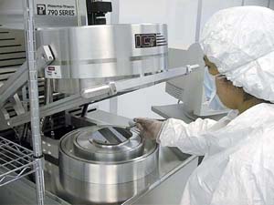
 Plasma
Science and Engineering Laboratories
Plasma
Science and Engineering LaboratoriesFacilities exist for fundamental plasma studies as well as research in novel plasma processing applications. Experiments in plasma waves and radiation use plasma chambers with wave detection systems. Microwave experiments include linear and reentrant cross field amplifiers designed for probe measurements. Other capabilities of the Plasma Science Laboratory are electron beam lithography, plasma ion implantation, and vacuum arc deposition. The Plasma Engineering Laboratory focuses on high-density inductively coupled plasmas (ICPs), plasma etching, and ionized physical vapor deposition. To aid in the investigation of plasma processes, the lab offers many diagnostic and measurement capabilities including rf-compensated Langmuir probes, quadrapole mass spectroscopy, optical emission spectroscopy, and microwave interferometry, as well as surface profilometry and scanning electron microscopy. Our goals are to study the fundamental aspects of dc, rf, and microwave plasmas, and to understand the interaction of these plasmas with the processing and production of novel electronic materials.
Complete facilities are available for producing and characterizing microwave materials and devices. Fabrication facilities include an ultra-high vacuum ion beam sputter deposition system and a thermal evaporation system. These facilities are designed for both oxide (e.g. high Tc superconductors) and metal thin films. Also available is a UHV magnetron sputtering system for triode-magnetron sputtering of elemental or YBaCuO targets. Characterization facilities include DC magnetization (VSM) and conductivity measurements, swept frequency ferromagnetic resonance, and millimeter-wave equipment.
An HP 8510B Automatic Network Analyzer is available for microwave measurements at frequencies up to 40 GHz using coaxial cables. Time domain and power spectrum measurements can be made with the microwave instrumentation available in the laboratory.
The VLSI Laboratory supports graduate research and undergraduate education in all areas of VLSI design and computer engineering. The facility houses over 25 networked workstations. (DEC station 3100+s and 5000+s) Viewlogic digital system CAD tools, XLynx field programmable gate arrays, and Berkley Magic/Oct VLSI CAD tool sets are available along with Kix, CalTech, WorkView and Cadence tools and several general event simulators. SUPREM III, SUPREM IV, and PISCES are used for process modeling and device simulation. A Tektronix ASIC tester is available. Fabrication is supported by MOSIS.
![]()

