Analog Integrated Circuit Design
Fall, 2019
Lab: 208 SN
Class Date & Time: Tuesday 5:10 pm to 6:20 pm or/and Wednedesday 5:00 pm to 6:30 pm
Instructor: Dr. Yong-Bin Kim (ybk@ece.neu.edu)
![]() TA: Gyunam Jeon (gjeon@ece.neu.edu)
TA: Gyunam Jeon (gjeon@ece.neu.edu)
Yixuan He (he.yix@husky.neu.edu )
Office hours: TBD (140 The Fenway R306)
Please check this web-page regularly. Don't be late to submit the report, and attend on your reserved date.
![]() Course Goals
Course Goals
![]() To study layouts of CMOS
combinational and sequential circuits.
To study layouts of CMOS
combinational and sequential circuits.![]() To utilize
switch-level and circuit-level simulators for the logic verification and timing
simulation.
To utilize
switch-level and circuit-level simulators for the logic verification and timing
simulation.
EECE 7420 must be taken concurrently.
![]() Course Grading
Course Grading
![]() Attendance
Attendance
![]() The correctness of the simulation
The correctness of the simulation
![]() The organization of the report (Student Laboratory
Report Format).
The organization of the report (Student Laboratory
Report Format).
![]() Confirm your
results with the TA before leaving.
Confirm your
results with the TA before leaving.
![]() Lab Section
Lab Section
![]() Section (Day & Hour : Tuesday 5:10 pm to 6:20 pm or/and Wednedesday 5:00 pm to 6:30 pm)
Section (Day & Hour : Tuesday 5:10 pm to 6:20 pm or/and Wednedesday 5:00 pm to 6:30 pm)
![]() One group has to consist of two students, and share one workstation with each other.
One group has to consist of two students, and share one workstation with each other.
![]() Each student has to submit a report. (Not a report per one group.)
Each student has to submit a report. (Not a report per one group.)
![]() Reference Materials for Lab
Reference Materials for Lab
![]() Cadence materials.
Cadence materials.
![]() Other References
Other References
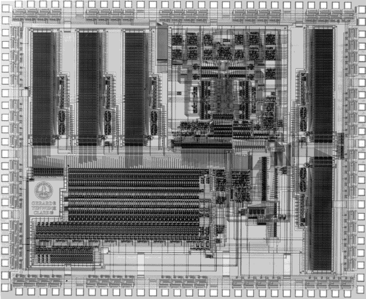
![]() IC Design Flow and Layout Example (These materials help you to understand the Circuit Layout)
IC Design Flow and Layout Example (These materials help you to understand the Circuit Layout)
![]() Lab Materials
Lab Materials
![]() Lab 0 (2 week) :
Tutorial Schematic
&
Tutorial Layout
Lab 0 (2 week) :
Tutorial Schematic
&
Tutorial Layout
Dr. Yong-Bin Kim. Department of Electrical and Computer Engineering![]() Lab 2 (1 week) : Lab #2 Guideline
Lab 2 (1 week) : Lab #2 Guideline
![]() Lab 3(1 week) : Lab #3 Guideline
Lab 3(1 week) : Lab #3 Guideline
![]() Lab 4 (1 week) : Lab #4 Guideline
Lab 4 (1 week) : Lab #4 Guideline
![]()
327 Dana Research Center, 360 Huntington Avenue, Boston, MA 02115, USA
Tel: (617) 373-2919, Fax: (617) 373-8970![]() ybk@ece.neu.edu
ybk@ece.neu.edu